Hole Types and classification
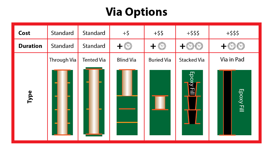
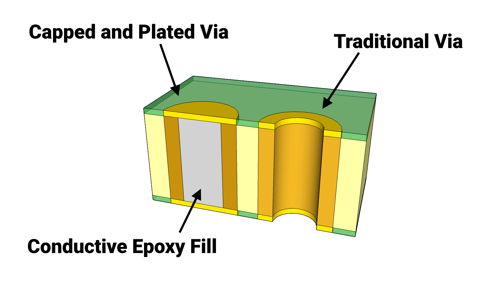
Vias are holes in the PCB strictly used as electrical paths connecting 2 or more layers of circuitry. Many processes allow the fiberglass between the copper planes to become conductive and thus platted copper bonds -- making a electrically functioning path.
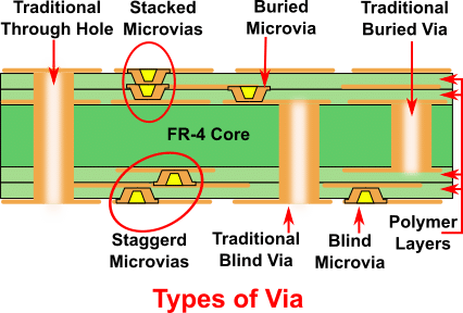
Through-Holes are drilled through the entire stack from the top layer, exiting through the bottom layer. When copper is plated to the fiber glass this allows the outermost layers and connecting inner layers to be electrically connected.
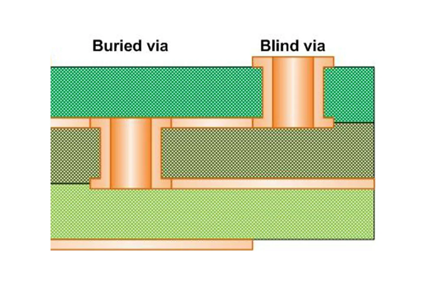
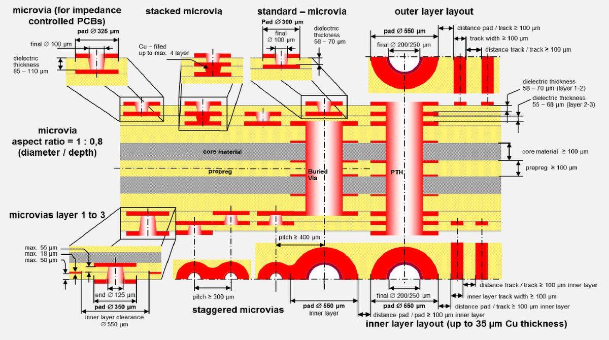
Blind Vias: Are started from either the top or bottom side or both sides in sequential steps. These vias are drilled at a 1:1 ratio maximum -- meaning a 10mil hole can only be drilled 10mils down otherwise trapped air can cause voids in the electrical path
Buried Vias: A single inner layer or a pressed group of inner-layers are drilled like a through-holes. The buried vias get copper plated and then filled with flowing resin from the subsequent press cycle.
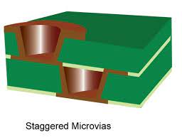
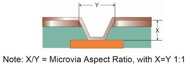
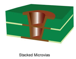
Micro Vias: Require a much higher technology for drilling using laser light at specific frequencies and pulse widths. The recipe for each hole size - depth - copper weight have to be adjusted precisely for flawless high density interconnect (HDI) utilizing this hole type. At Miltec Circuits we have perfected this method and have many years experience in the field of HDI PCBs
 IPC-4761
Please see Design Guide for Protection of Printed Board Via Structures →